Primarily, electronics are divided into two parts:
electronic components
the printed circuit board
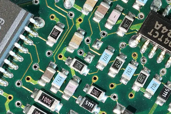
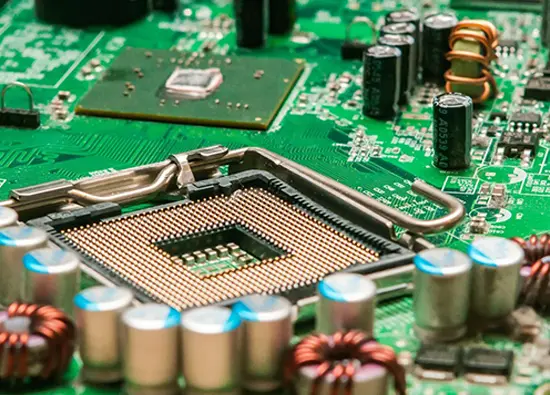
Electronic components are elements designed to be linked together to perform one or more specific electronic functions. They can be separated into different types and categories, including: sensors (cameras, thermocouples, etc.), power electronics (fuses, relays, etc.), analogue electronics (capacitors, diodes, resistors, transistors, etc.), digital electronics (microprocessor, microcontroller, etc.) and man-machine interfaces (displays, loudspeakers, LEDs, etc.). Their assembly must first be defined by an electrical diagram.
Figure 1: Electronic components
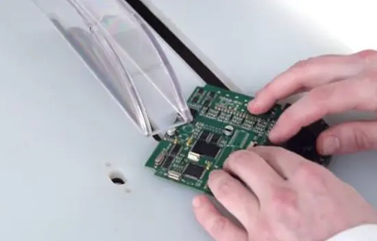
A Printed Circuit Board (PCB) is a substrate, usually in the form of a board, made from composite materials. The purpose of this support is to electrically connect a set of electronic components in order to create an electronic circuit.
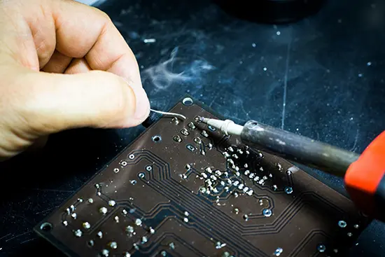
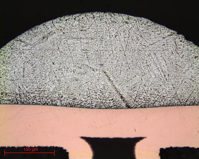
Electronic components are soldered onto the printed circuit board. This operation is called “brazing” which, unlike soldering, allows the components to be assembled without melting. Brazing only melts the filler metal, and that ensures continuity between the components.
The filler metal is different from that of the parts to be joined and is therefore chosen according to the material of the parts and the type of brazing to be carried out. In the world of electronics brazing is mainly performed using tin alloys.
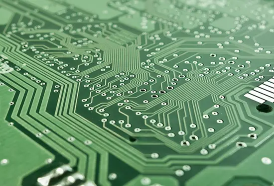
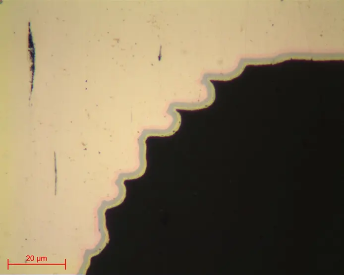
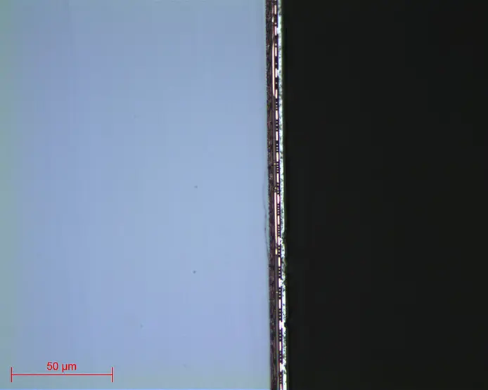
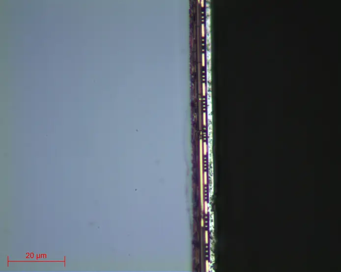
The printed circuit board is made from insulating epoxy resin separated into several thicknesses by thin layers of copper. Copper ensures the passage of electric current, thus creating electrical circuits. As the number of layers has increased exponentially over time, printed circuits have become increasingly complex and efficient. The different layers are connected by metallised holes (by copper deposition) called “via holes”. Printed circuits are very often covered with a thin layer of varnish to protect them from corrosion.
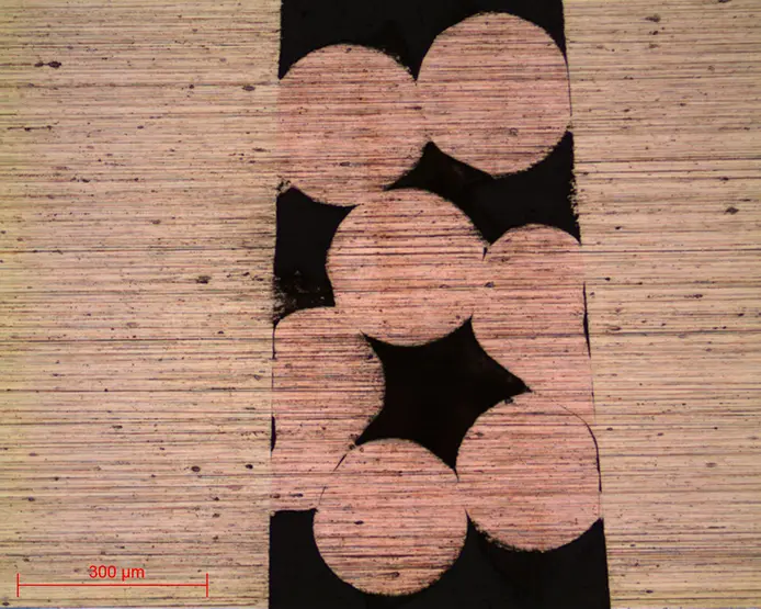
Figure 3: Printed circuit board and illustration of metallised via holes
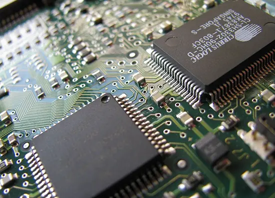
An electronic circuit is a set of electronic components connected to each other on a printed circuit board whose purpose is to perform one or more functions.
Figures 4 & 5: Electronic circuits
2 CONNECTIONS
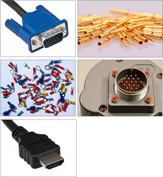
An extension of the subject of electronic circuits is “connection technology”. Connectivity corresponds to all the techniques relating to electrical connections and data transmission, i.e. the various connectors and sockets.
There are several categories of connectors: electrotechnical connectors (electrical sockets, power supply, terminals, terminal blocks or “dominoes”, etc.), electronic pins, computer connectors, audio (JACK, DIN, SPEAKON, etc.) and video connectors (HDMI, VGA, DVI, etc.) or so-called “professional” connectors (MIL-DTL- 38999, DBAS, BNC-TNC, etc.).
METALLOGRAPHIC PREPARATION
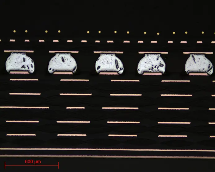
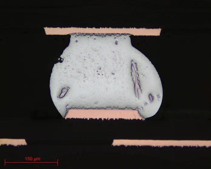
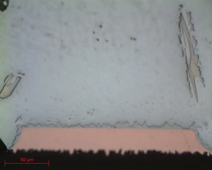
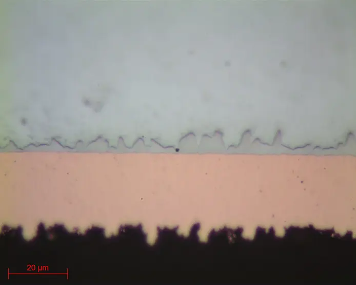
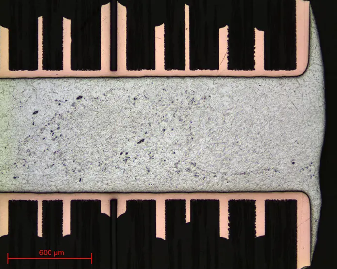
Whether electronic circuits or connector parts, quality controls must be carried out throughout the production process. In general, the priorities are to check brazing, electrical contacts between the various components and the printed circuit board, metallisation quality, dimensional characteristics, coating thickness, etc.
The main materials found in the field of electronics are:
Metals with excellent electrical conductivity or coatings such as copper, silver, nickel and gold,
Tin alloys for soldering,
Polymers for printed circuit boards and electronic modules,
The glass and ceramics (and silicon) that make up the various components.
Inspection requires metallographic preparation. Obtaining an inspection surface requires a succession of operations, each as important as the next, regardless of the material.
These steps are in the following order:
The removal of the product to be examined (if necessary), called “CUTTING”.
Standardisation of the geometry of the sample taken (if necessary), called “MOUNTING”.
Improvement of the surface condition of this sample, called “POLISHING”.
Characterisation of the sample: revealing the microstructure of the sample by an etching reagent (if necessary) called “METALLOGRAPHIC ETCHING” and microscopic observation (optical or electronic).
=> Each of these steps must be carried out rigorously, otherwise the following steps will not be possible.
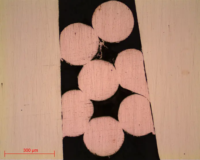
The purpose of cutting is to remove a precise section of a product, in order to obtain a suitable surface for inspection, without altering the physico-chemical properties of the electronic parts.
In other words, it is essential to avoid heating, deformation or excessive aggressiveness of the cut, which can lead to many different types of damage (cracks/spalling of components, detachment of coatings/metallisations, etc.) to the areas to be inspected. Cutting is a fundamental step which conditions the further preparation and inspection of parts.
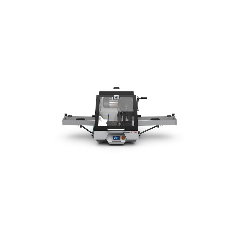
PRESI’s wide range of medium and large capacity cutting and micro-cutting machines, and also the range of WELL diamond wire saws, can be adapted to any need with regard to cutting precision, sizing or quantity of products to be cut:
Each cutting machine and wire saw is equipped with the appropriate consumables and accessories. The clamping system and the choice of these consumables are always essential elements for the success of a metallographic cut.
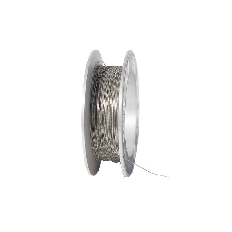
The choice of machine type depends on the geometry of the workpieces to be cut and their sensitivity/fragility, as the clamping possibilities differ. The advantage of wire saws is that they use low support forces which are gentle on the specimens. They also provide very good surface finishes but have longer cutting times.
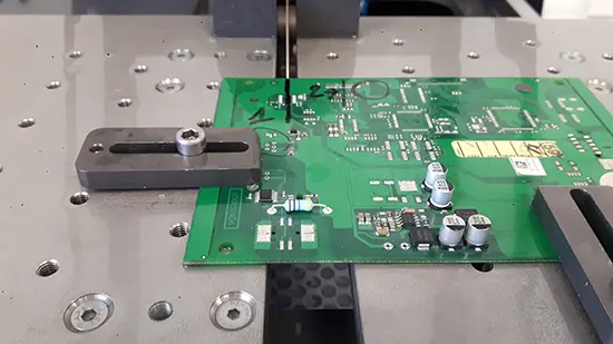
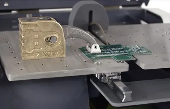
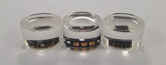
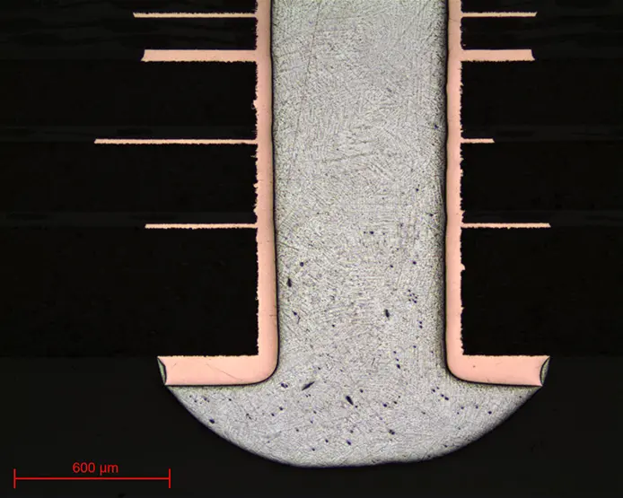
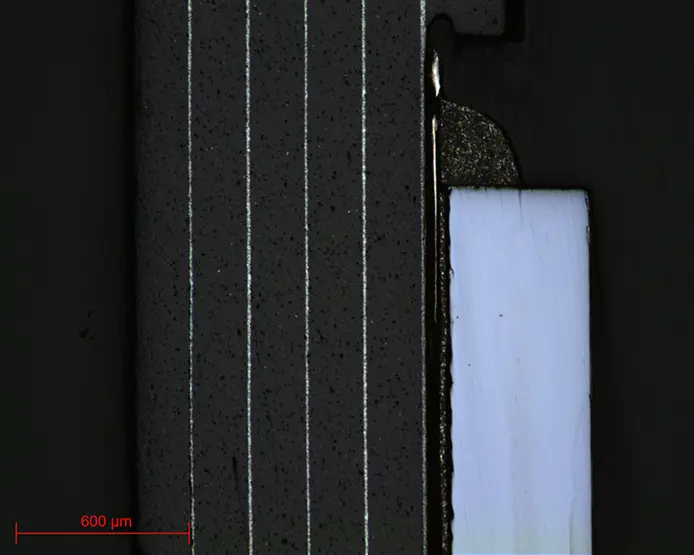
Figure 11: Example of clamping of an electronic circuit – FLEXICUT
Figures 12: Example of clamping of an electronic circuit – FLEXICUT
Figures 13: Example of clamping of an electronic circuit – FLEXICUT
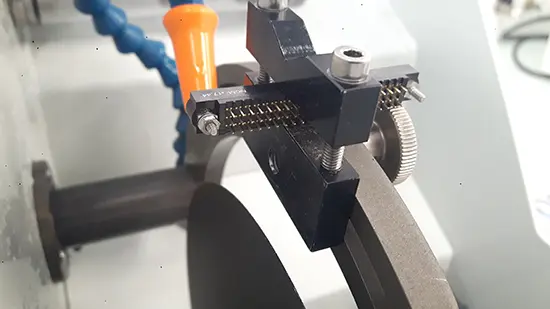
Figure 14: Example of clamping a connector MECATOME T202
Figures 15 & 16: Examples of clamping and electronic connector 4000 series wire saw
All cutting machines are used with a lubricating/cooling liquid composed of a mixture of water and anti-rust additive in order to obtain a clean cut without overheating. The additive also protects the sample and the machine from corrosion.
Wire saws, on the other hand, are used with a cutting fluid that acts as a lubricant and “cleaner” that extends the life of the wire and allows a better quality of cut to be achieved.
SOFT METALS (Copper, Tin, Gold, Silver, etc.)
PLASTICS AND POLYMERS
CERAMICS
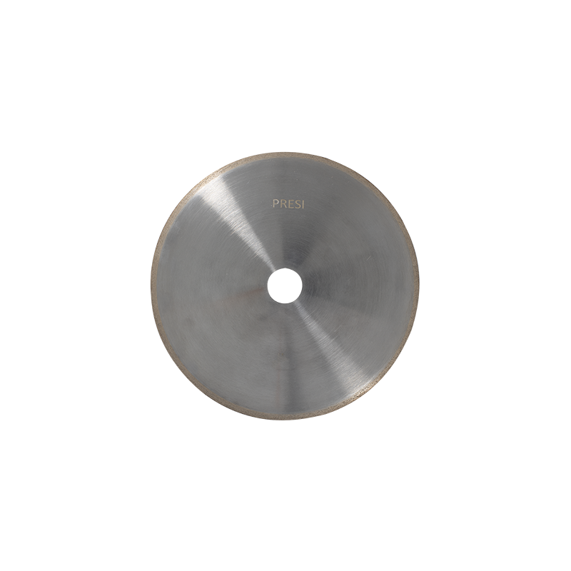
Micro-cutting
UTW S Ø180
UTW S Ø180mm LM+ LR
LM+
LR
Medium-capacity cutting
MNF T
MNF LM+ LR
LM+ LR
Table 1: Choosing the right cut-off wheel type according to the main material of the electronic part
=> The choice of the cut-off wheel type has to be adequate, in order to avoid cutting failure, or excessive cut-off wheel wear or even breakage. The hardness of the workpiece determines the wheel selection.
The consumables available for wire saws are stainless steel wires set with diamonds. The characteristics of the wires vary according to requirements and needs. The range is comprised of seven wire diameters from 0.1-0.7 mm and five diamond grit sizes from 20-64μm.
MOUNTING
Samples can be difficult to handle due to their complex shape, fragility or small size. Mounting makes them easier to handle by standardising their geometry and dimensions.
=> Achieving good-quality mounting is essential to protect fragile materials and also to achieve good preparation results for polishing and future analysis.
There are two mounting options: hot or cold mounting. In electronics it is always preferable to use the cold mounting since very often the parts are fragile and therefore unsuitable for high pressures, and they are probably also sensitive to heat.
LE PROCÉDÉ À FROID
It can use two devices aimed at considerably improving quality, in particular by redu- cing shrinkage (gap between the resin and the sample), optimising transparency or facilitating resin impregnation.
+ POINT
Substantially improves quality, in particular by reducing shrinkage, optimising transparency and facilitating resin impregnation.
Other advantages of cold mounting include the impregnation quality of the resins, perfect for porous samples, and the possibility of mass production mounting.
CONSUMABLES
In electronics, metallographic preparation absolutely requires the use of a transparent resin. This transparency allows a constant view of the sample and thus precise knowledge of the observation plane.
MICRO-ELECTRONICS
CONNECTION TECHNOLOGY
Cold process
Pressurized acrylic KM-U Hot
Epoxy IP
MA2+
2S*
Table 2: Choosing the right mounting resin type
* Suitable for very large series
The use of KM-U acrylic resin requires a “pressure embedding device” to ensure transparency. The pressure helps to expel air bubbles in the liquid resin and reduces shrinkage.
=> This resin has the advantage of a short curing time (15 minutes) and also presents very good hardness.
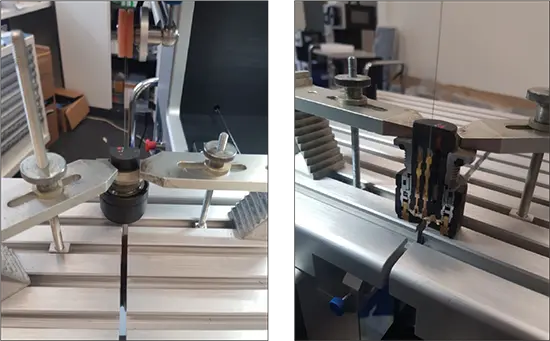
Figure 19: Coating with the use of “pressure coating equipment”
IP epoxy resin has a longer curing time (8 hours) and does not rise in temperature above 30°C. It also allows better impregnation if polymerisation takes place under vacuum using “Poly’Vac”.
POLISHING
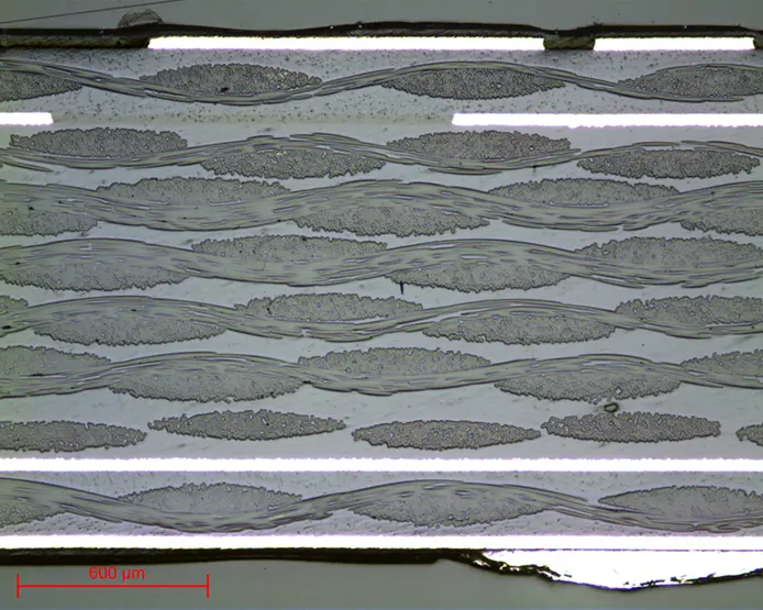
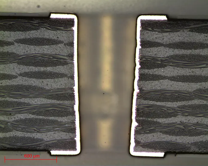
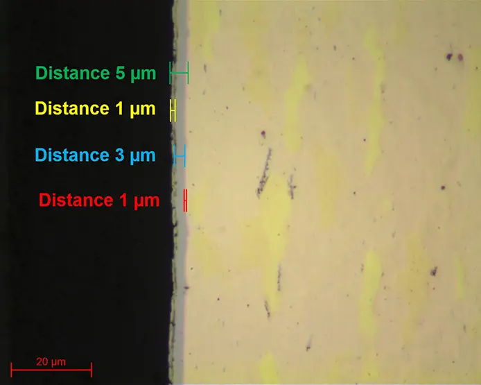
The last and crucial phase in the sample preparation process is polishing. The principle is simple, each step uses a finer abrasive than the previous one. The aim is to obtain a flat surface and to eliminate scratches and residual defects that would hinder the performance of metallographic control examinations such as microscopic analysis, hardness tests, microstructure or dimensional inspections.
PRESI offers a wide range of manual and automatic polishing machines, with a wide choice of accessories, to cover all needs, from pre-polishing to super-finishing and polishing of single or series samples.
The aim of metallographic preparation of connector or microelectronic samples is often to reach and observe very precise areas of the parts. Therefore, polishing must be carried out in the most controlled manner possible. Manual polishing is therefore more advisable.
All the polishing ranges below are given for automatic specimen preparation (for manual polishing: do not take into account the parameters at the top). They are the most commonly used and are given for information and advice.
=> All the first steps of each range are called “levelling” and consist of removing material quickly to level the surface of the specimen (and resin). Those given below are standard and can therefore be modified as required. In practice, the aim is to reach the area of the sample to be studied after the pre-polishing steps. In this way the polishing is carried out directly on the components to be inspected.
Applied pressures vary according to sample size, but in general the following applies: 1daN per 10mm mounting diameter for the pre-polishing steps (ex: Ø40mm = 4 daN) then reduce force by 0.5daN at each polishing step with an abrasive suspension.
RANGE N°1
N°
Support
Suspension / Lubricant
Platen Speed (RPM)
Head Speed (RPM)
Rotation direction platen / head
Time
1
SiC P320
Ø / Water
300
150
→ →
1’
2
SiC P1200
Ø / Water
300
150
→ →
1’
3
RAM
3μm LDM / Reflex Lub
150
135
→ →
3’
4
NT
3µm LDP / Reflex Lub
150
135
→ →
1’
5
SUPRA
(SPM) / Water
150
100
→ ←
1’
Range N°1 is optimised for examining soft materials within a microelectronics or connector sample. It is perfectly suitable for solders made of tin alloys, metallic components (copper, silver, gold, nickel, brass, etc.), polymers (resin, rubber, casings, etc.), or varnish.
RANGE N°2
N°
Support
Suspension / Lubricant
Platen Speed (RPM)
Head Speed (RPM)
Rotation direction platen / head
Time
1
Tissediam 40μm
Ø / Water
300
150
→ →
2’
2
Tissediam 20μm
Ø / Water
300
150
→ →
2’
3
TOP
9μm LDP / Reflex Lub
150
135
→ →
5’
4
RAM
3μm LDP / Reflex Lub
150
135
→ →
2’
5
SUPRA
SPM / Water
150
100
→ ←
2’
Range No. 2 is optimised for the inspection of ceramic components. If the specimen to be exa- mined consists mainly of ceramics, then the hardness differentials within the same specimen are very high. In this case, consumables must be adapted to ensure homogeneous material removal regardless of hardness. This is the role of metal bonded diamond discs called “TISSEDIAM”.
More generally, an “electronics” sample is made up of a multitude of different materials. There is therefore a risk of creating unevenness between the different components during polishing, causing difficulties during observation.
Sometimes, it is not necessary to carry out the polishing range up to super-finishing, particularly in the case of crimping controls, dimensioning or any other inspections on large connector samples.
However finishing must be performed with colloidal silica in the last polishing stage to observe the finest components, intermetallics, porosity brazing, etc…